Miniaturisation
At the end of the previous gameboy post we ended up with a gameboy driving a modern TFT LCD, complete with pixel art upscaling in hardware. The problem though is that the various development boards are a long way from fitting in the gameboy case. I really wanted a neat solution that fits inside the original case without having to hack it about. Now that the original gameboy is a 30 year old antique, that would feel like vandalism.
FPGA
The prototype used a Xilinx Spartan 3 which, while an old product, is overkill for this project. My design only uses about 10% of the Spartan 3 logic resources and it would comfortably run at over 100MHz without even attempting any optimization. Not only is the Spartan FPGA overkill, it is relatively complicated to use in that it needs an external PROM to store the configuration and three separate voltage rails. Xilinx & Intel both seem to leave the low-end of the FPGA market to their smaller competitors, so I chose a Lattice FPGA for this project. The MX02-1200 is the lowest end FPGA that has block RAM (needed for the pixel buffer) and comes in a tiny 32 pin CFP package which integrates the PROM and needed voltage regulators.
Custom PCB
There is no getting away from the fact that a custom PCB is needed to pull this off. The space for the old LCD is a little plastic frame about 50x45x5mm. Thankfully, high quality custom PCBs are now well within the grasp of the hobbyist. I used DirtyPCB this time and found the quality to be excellent although the cheap postage can be hit and miss (it took 6 weeks in this case). The FedEx shipping is fast but they sting you for customs clearance fees. There simply is no point mucking around with veroboard anymore, especially if you value your time and/or want to use dense surface mount components (like the FPGA I’ve chosen and the LCD itself).
Below is a picture of the PCB layout, looking from underneath with red being the bottom-side copper and green the top-side. U1 is a 3.3V regulator that steps down the gameboy 5V to the 3.3V needed to power the LCD and FPGA. U2 is the FPGA itself. U3 is an octal buffer used to level shift from the 5V logic of the gameboy to the 3.3V IO of the FPGA. The row of pads on the top-side of the board (green) are directly soldered to the flex coming from the LCD. J3 is the JTAG connector for programming the FPGA.
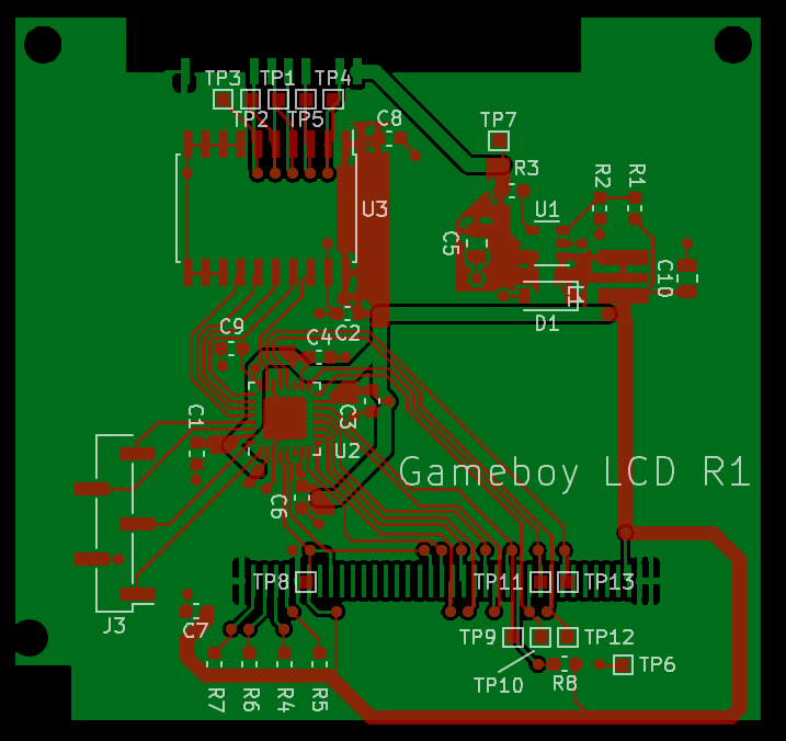
It’s not a great PCB layout, it shows what you can get away with for a one-off low-speed design that doesn’t need to go through any sort of EMC testing. I highly recommend this textbook if you’re interested in the subject.
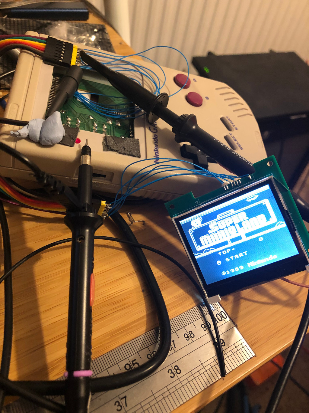
First working prototype
The below picture shows the assembled PCB working for the first time. There was a bug in the upscaling at this point where it was reading/writing the same row in the buffer at the same time, so the image quality isn’t as good as it should be.
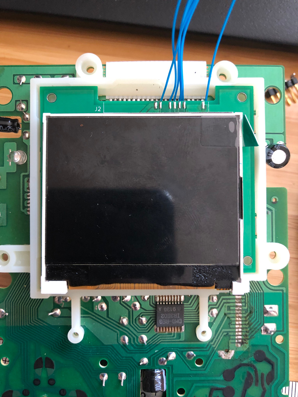
Mid surgery
At this point you can see how the PCB fits exactly inside the plastic frame that housed the original LCD. I’m using wire wrap wires (bodge wires!) to wire from the gameboy ribbon connector to pads on the PCB. There are seven connections - GND, VCC, HSYNC, VSYNC, CLK and the two DATA lines.
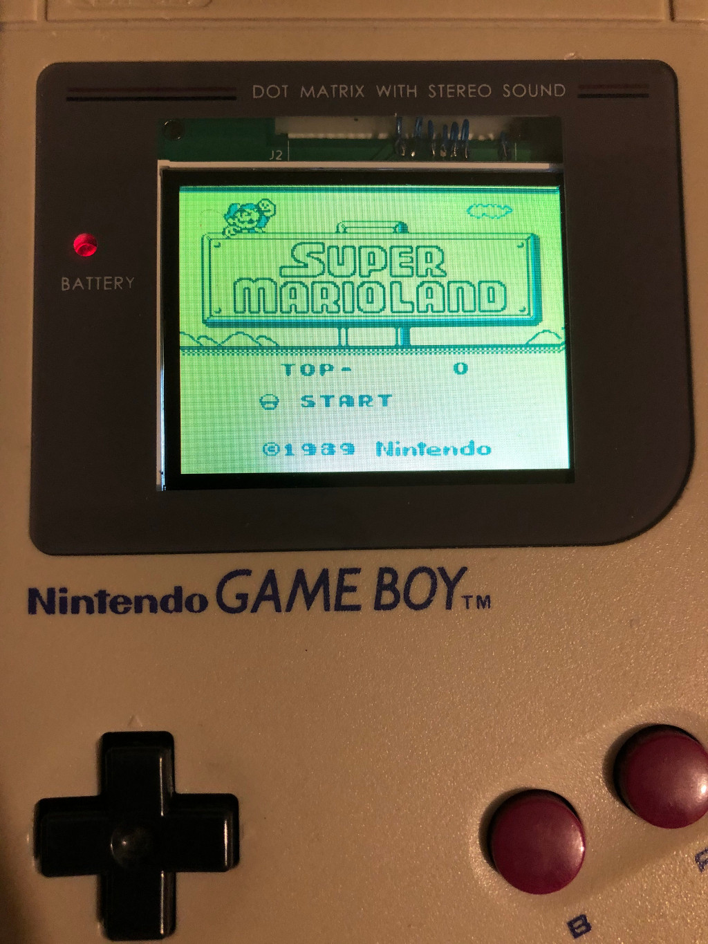
Complete!
All back together! At this point the upscaling bug has been fixed and I’ve changed the colour scheme to a retro one that mimics the original LCD. I’ve not been able to assess the impact on battery life yet, the backlight is surely going to consume more power than the original LCD. So far I’ve managed a few hours of play on the same set of batteries, so it’s definitely not terrible. If I wanted to optimize then a proper LED driver with brightness adjustment (vs current-limiting resistors) would be the place to start.
Source code
Try it yourself! Verilog source code for the FPGA available on github.